
Solar Power from Space? Caltech’s $100 Million Gambit
Nonetheless, when computer system chips is not going to burn up a literal hole in your pocket (while they do get scorching adequate to
fry an egg), they even now demand a whole lot of current to operate the applications we use just about every day. Contemplate the data-centre SoC: On ordinary, it truly is consuming two hundred W to present its transistors with about one to two volts, which means the chip is drawing one hundred to two hundred amperes of current from the voltage regulators that offer it. Your normal fridge draws only six A. Superior-close cell phones can draw a tenth as a great deal electrical power as data-centre SoCs, but even so that’s even now about 10–20 A of current. Which is up to a few refrigerators, in your pocket!
Providing that current to billions of transistors is promptly becoming one of the major bottlenecks in superior-performance SoC design and style. As transistors go on to be manufactured tinier, the interconnects that offer them with current should be packed at any time nearer and be manufactured at any time finer, which boosts resistance and saps electrical power. This are unable to go on: Devoid of a massive improve in the way electrons get to and from units on a chip, it is not going to issue how a great deal smaller sized we can make transistors.
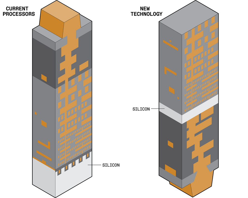
In present-day processors both equally alerts and electrical power achieve the silicon [light grey] from above. New technology would separate these functions, saving electrical power and producing a lot more space for signal routes [proper].Chris Philpot
Fortunately, we have a promising remedy: We can use a side of the silicon that’s very long been dismissed.
Electrons have to journey a very long way to get from the source that is building them to the transistors that compute with them. In most electronics they journey along the copper traces of a printed circuit board into a bundle that retains the SoC, by way of the solder balls that hook up the chip to the
bundle, and then via on-chip interconnects to the transistors themselves. It can be this very last phase that genuinely issues.
To see why, it assists to understand how chips are manufactured. An SoC starts as a bare piece of superior-top quality, crystalline silicon. We initially make a layer of transistors at the pretty major of that silicon. Subsequent we url them collectively with metal interconnects to sort circuits with helpful computing functions. These interconnects are shaped in levels named a stack, and it can just take a 10-to-twenty-layer stack to produce electrical power and data to the billions of transistors on present-day chips.
These levels closest to the silicon transistors are slender and modest in purchase to hook up to the tiny transistors, but they mature in dimension as you go up in the stack to greater ranges. It can be these ranges with broader interconnects that are much better at offering electrical power simply because they have less resistance.
Nowadays, both equally electrical power and alerts achieve transistors from a community of interconnects above the silicon (the “entrance side”). But escalating resistance as these interconnects are scaled down to at any time-finer dimensions is producing that scheme untenable.Chris Philpot
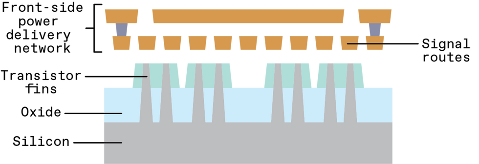
You can see, then, that the metal that powers circuits—the electrical power shipping and delivery community (PDN)—is on major of the transistors. We refer to this as entrance-side electrical power shipping and delivery. You can also see that the electrical power community unavoidably competes for area with the community of wires that delivers alerts, simply because they share the same established of copper means.
In purchase to get electrical power and alerts off of the SoC, we commonly hook up the uppermost layer of metal—farthest away from the transistors—to solder balls (also named bumps) in the chip bundle. So for electrons to achieve any transistor to do helpful get the job done, they have to traverse 10 to twenty levels of increasingly slender and tortuous metal until eventually they can eventually squeeze by way of to the pretty very last layer of regional wires.
This way of distributing electrical power is basically lossy. At just about every phase along the route, some electrical power is shed, and some should be applied to regulate the shipping and delivery itself. In present-day SoCs, designers commonly have a spending budget that will allow decline that prospects to a 10 percent reduction in voltage amongst the bundle and the transistors. As a result, if we hit a total efficiency of 90 percent or increased in a electrical power-shipping and delivery community, our styles are on the proper observe.
Historically, this kind of efficiencies have been achievable with very good engineering—some could possibly even say it was quick in comparison to the issues we face nowadays. In present-day electronics, SoC designers not only have to handle escalating electrical power densities but to do so with interconnects that are getting rid of electrical power at a sharply accelerating fee with each new technology.
You can design and style a back-side electrical power shipping and delivery community that’s up to seven periods as efficient as the standard entrance-side community.
The escalating lossiness has to do with how we make nanoscale wires. That approach and its accompanying supplies trace back to about 1997, when IBM began to make interconnects out of copper alternatively of aluminum, and the business shifted along with it. Up until eventually then aluminum wires experienced been good conductors, but in a number of a lot more methods along the
Moore’s Law curve their resistance would shortly be too superior and turn into unreliable. Copper is a lot more conductive at fashionable IC scales. But even copper’s resistance began to be problematic after interconnect widths shrank below one hundred nanometers. Nowadays, the smallest produced interconnects are about twenty nm, so resistance is now an urgent concern.
It assists to photo the electrons in an interconnect as a entire established of balls on a billiards table. Now imagine shoving them all from one close of the table toward another. A number of would collide and bounce towards each other on the way, but most would make the journey in a straight-ish line. Now consider shrinking the table by half—you’d get a whole lot a lot more collisions and the balls would move a lot more gradually. Subsequent, shrink it again and increase the selection of billiard balls tenfold, and you happen to be in anything like the condition chipmakers face now. True electrons do not collide, automatically, but they get shut adequate to one another to impose a scattering drive that disrupts the circulation by way of the wire. At nanoscale dimensions, this prospects to vastly greater resistance in the wires, which induces considerable electrical power-shipping and delivery decline.
Growing electrical resistance is not a new challenge, but the magnitude of increase that we are seeing now with each subsequent approach node is unprecedented. In addition, standard means of taking care of this increase are no for a longer time an option, simply because the production rules at the nanoscale impose so quite a few constraints. Absent are the times when we could arbitrarily increase the widths of particular wires in purchase to beat escalating resistance. Now designers have to adhere to particular specified wire widths or else the chip may perhaps not be manufacturable. So, the business is confronted with the twin complications of greater resistance in interconnects and less space for them on the chip.
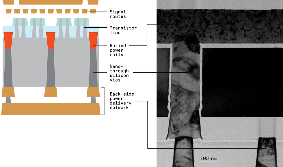
There is another way: We can exploit the “vacant” silicon that lies below the transistors. At Imec, exactly where authors Beyne and Zografos get the job done, we have pioneered a production concept named “buried electrical power rails,” or BPR. The system builds electrical power connections below the transistors alternatively of above them, with the aim of producing fatter, less resistant rails and liberating area for signal-carrying interconnects above the transistor layer.
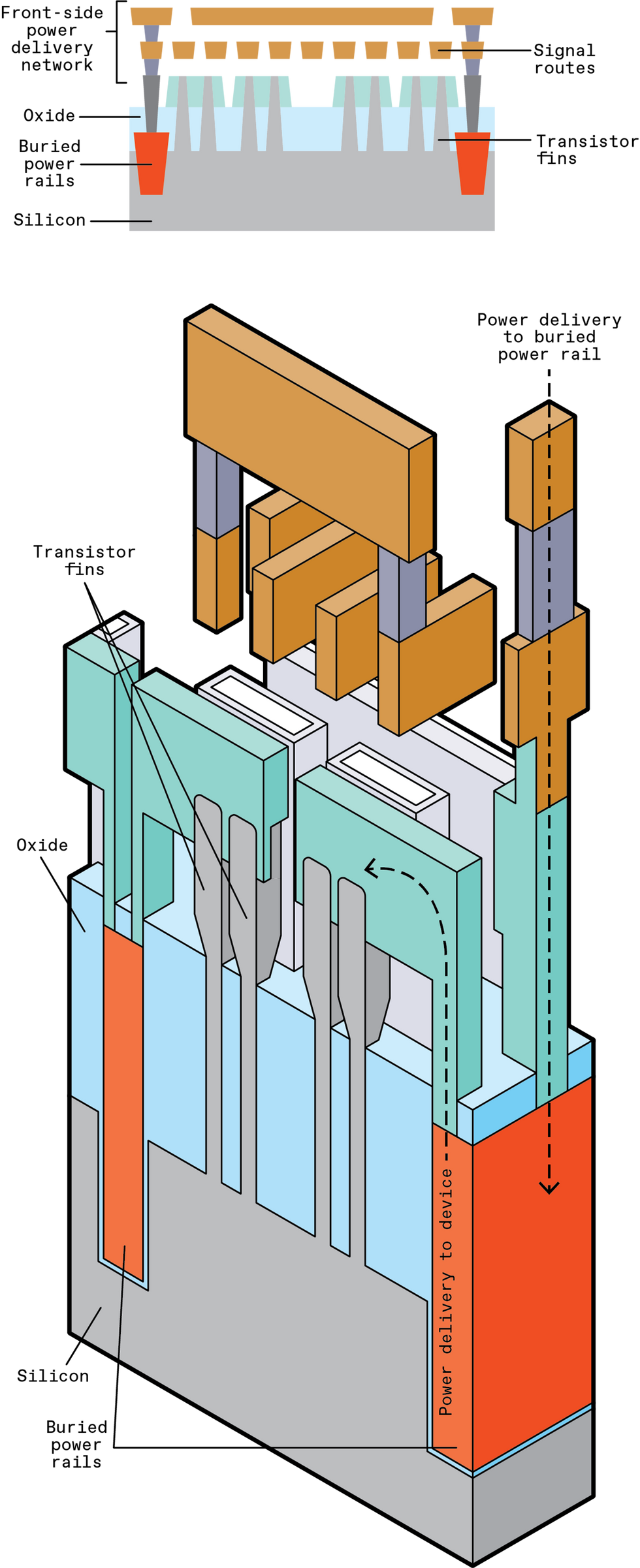
To lessen the resistance in electrical power shipping and delivery, transistors will faucet electrical power rails buried in the silicon. These are fairly significant, low-resistance conductors that many logic cells could hook up with.Chris Philpot
To create BPRs, you initially have to dig out deep trenches below the transistors and then fill them with metal. You have to do this prior to you make the transistors themselves. So the metal selection is critical. That metal will need to have to endure the processing methods applied to make superior-top quality transistors, which can achieve about one,000 °C. At that temperature, copper is molten, and melted copper could contaminate the complete chip. We have therefore experimented with ruthenium and tungsten, which have greater melting points.
Considering that there is so a great deal unused area below the transistors, you can make the BPR trenches extensive and deep, which is perfect for offering electrical power. In contrast to the slender metal levels instantly on major of the transistors,
BPRs can have one/twenty to one/30 the resistance. That means that BPRs will properly enable you to produce a lot more electrical power to the transistors.
In addition, by moving the electrical power rails off the major side of the transistors you no cost up space for the signal-carrying interconnects. These interconnects sort fundamental circuit “cells”—the smallest circuit models, this kind of as SRAM memory bit cells or simple logic that we use to compose a lot more elaborate circuits. By using the area we’ve freed up, we could shrink these cells by
sixteen percent or a lot more, and that could in the end translate to a lot more transistors for each chip. Even if feature dimension stayed the same, we would even now force Moore’s Law one stage even further.
Regrettably, it looks like burying regional electrical power rails on your own is not going to be adequate. You even now have to express electrical power to these rails down from the major side of the chip, and that will expense efficiency and some decline of voltage.
Absent are the times when we could arbitrarily increase the widths of particular wires in purchase to beat escalating resistance.
Scientists at Arm, which includes authors Cline and Prasad, ran a simulation on one of their CPUs and uncovered that, by themselves, BPRs could enable you to create a 40 percent a lot more efficient electrical power community than an regular entrance-side electrical power shipping and delivery community. But they also uncovered that even if you applied BPRs with entrance-side electrical power shipping and delivery, the in general voltage sent to the transistors was not superior adequate to sustain superior-performance operation of a CPU.
Luckily for us, Imec was at the same time acquiring a complementary remedy to even further strengthen electrical power shipping and delivery: Move the entire electrical power-shipping and delivery community from the entrance side of the chip to the back side. This remedy is named “back-side electrical power shipping and delivery,” or a lot more generally “back-side metallization.” It will involve thinning down the silicon that is underneath the transistors to 500 nm or less, at which place you can create nanometer-dimension “by way of-silicon vias,” or
nano-TSVs. These are vertical interconnects that can hook up up by way of the back side of the silicon to the base of the buried rails, like hundreds of tiny mineshafts. When the nano-TSVs have been established below the transistors and BPRs, you can then deposit further levels of metal on the back side of the chip to sort a entire electrical power-shipping and delivery community.
Expanding on our earlier simulations, we at Arm uncovered that just two levels of thick back-side metal was adequate to do the occupation. As very long as you could area the nano-TSVs nearer than two micrometers from each other, you could design and style a back-side PDN that was four periods as efficient as the entrance-side PDN with buried electrical power rails and seven periods as efficient as the standard entrance-side PDN.
The back-side PDN has the further advantage of being bodily divided from the signal community, so the two networks no for a longer time contend for the same metal-layer means. You can find a lot more space for each. It also means that the metal layer features no for a longer time need to have to be a compromise amongst what electrical power routes want (thick and extensive for low resistance) and what signal routes want (slender and slender so they can make circuits from densely packed transistors). You can at the same time tune the back-side metal levels for electrical power routing and the entrance-side metal levels for signal routing and get the finest of both equally worlds.
Going the electrical power shipping and delivery community to the other side of the silicon—the “back side”—reduces voltage decline even a lot more, simply because all the interconnects in the community can be manufactured thicker to decreased resistance. What’s a lot more, taking away the electrical power-shipping and delivery community from above the silicon leaves a lot more space for signal routes, primary to even smaller sized logic circuits and permitting chipmakers squeeze a lot more transistors into the same space of silicon.
Chris Philpot/IMEC
In our styles at Arm, we uncovered that for both equally the standard entrance-side PDN and entrance-side PDN with buried electrical power rails, we experienced to sacrifice design and style performance. But with back-side PDN the CPU was equipped to reach superior frequencies
and have electrically efficient electrical power shipping and delivery.
You could possibly, of training course, be thinking how you get alerts and electrical power from the bundle to the chip in this kind of a scheme. The nano-TSVs are the important below, too. They can be applied to transfer all input and output alerts from the entrance side to the back side of the chip. That way, both equally the electrical power and the I/O alerts can be attached to solder balls that are placed on the back side.
Simulation experiments are a good get started, and they display the CPU-design and style-level potential of back-side PDNs with BPR. But there is a very long street ahead to deliver these technologies to superior-quantity production. There are even now considerable supplies and production issues that need to have to be solved. The finest selection of metal supplies for the BPRs and nano-TSVs is significant to manufacturability and electrical efficiency. Also, the superior-facet-ratio (deep but skinny) trenches wanted for both equally BPRs and nano-TSVs are pretty hard to make. Reliably etching tightly spaced, deep-but-slender characteristics in the silicon substrate and filling them with metal is fairly new to chip manufacture and is even now anything the business is finding to grips with. Creating production equipment and approaches that are responsible and repeatable will be essential to unlocking widespread adoption of nano-TSVs.
In addition, battery-driven SoCs, like these in your mobile phone and in other electrical power-constrained styles, already have a great deal a lot more refined electrical power-shipping and delivery networks than these we’ve discussed so considerably. Modern day-day electrical power shipping and delivery separates chips into many electrical power domains that can run at unique voltages or even be turned off entirely to preserve electrical power. (See ”
A Circuit to Boost Battery Lifestyle,” IEEE Spectrum, August 2021.)
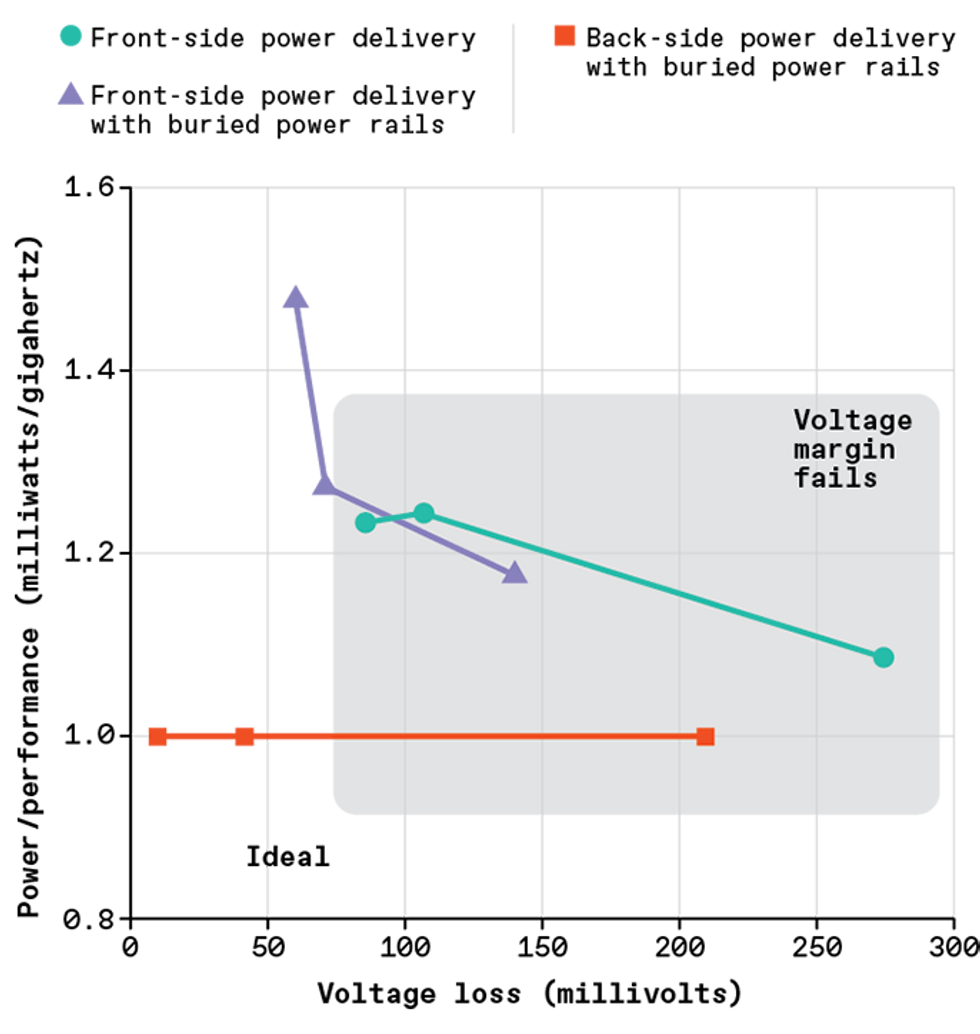
In assessments of many styles using a few kinds of electrical power shipping and delivery, only back-side electrical power with buried electrical power rails [purple] gives adequate voltage devoid of compromising performance.Chris Philpot
As a result, back-side PDNs and BPRs are inevitably likely to have to do a great deal a lot more than just effectively produce electrons. They’re likely to have to exactly regulate exactly where electrons go and how quite a few of them get there. Chip designers will not want to just take many methods backward when it arrives to chip-level electrical power design and style. So we will have to at the same time enhance design and style and production to make confident that BPRs and back-side PDNs are much better than—or at minimum appropriate with—the electrical power-saving IC procedures we use nowadays.
The future of computing relies upon upon these new production procedures. Electricity use is essential regardless of whether you happen to be worrying about the cooling bill for a data centre or the selection of periods you have to cost your smartphone each day. And as we go on to shrink transistors and ICs, offering electrical power turns into a considerable on-chip challenge. BPR and back-side PDNs may perhaps nicely response that challenge if engineers can triumph over the complexities that come with them.
This short article seems in the September 2021 print concern as “Electricity From Down below.”


