
General Fusion Takes Aim at Practical Fusion Power
Nonetheless, though computer system chips will not likely burn up a literal hole in your pocket (however they do get sizzling more than enough to
fry an egg), they continue to need a ton of latest to operate the applications we use every day. Think about the data-centre SoC: On typical, it truly is consuming 200 W to provide its transistors with about one to 2 volts, which usually means the chip is drawing one hundred to 200 amperes of latest from the voltage regulators that provide it. Your standard refrigerator draws only 6 A. High-conclusion cellular phones can attract a tenth as considerably power as data-centre SoCs, but even so which is continue to about 10–20 A of latest. That’s up to three fridges, in your pocket!
Delivering that latest to billions of transistors is rapidly getting to be one particular of the key bottlenecks in significant-functionality SoC structure. As transistors keep on to be designed tinier, the interconnects that provide them with latest will have to be packed ever closer and be designed ever finer, which will increase resistance and saps power. This won’t be able to go on: Devoid of a big adjust in the way electrons get to and from products on a chip, it will not likely subject how considerably scaled-down we can make transistors.
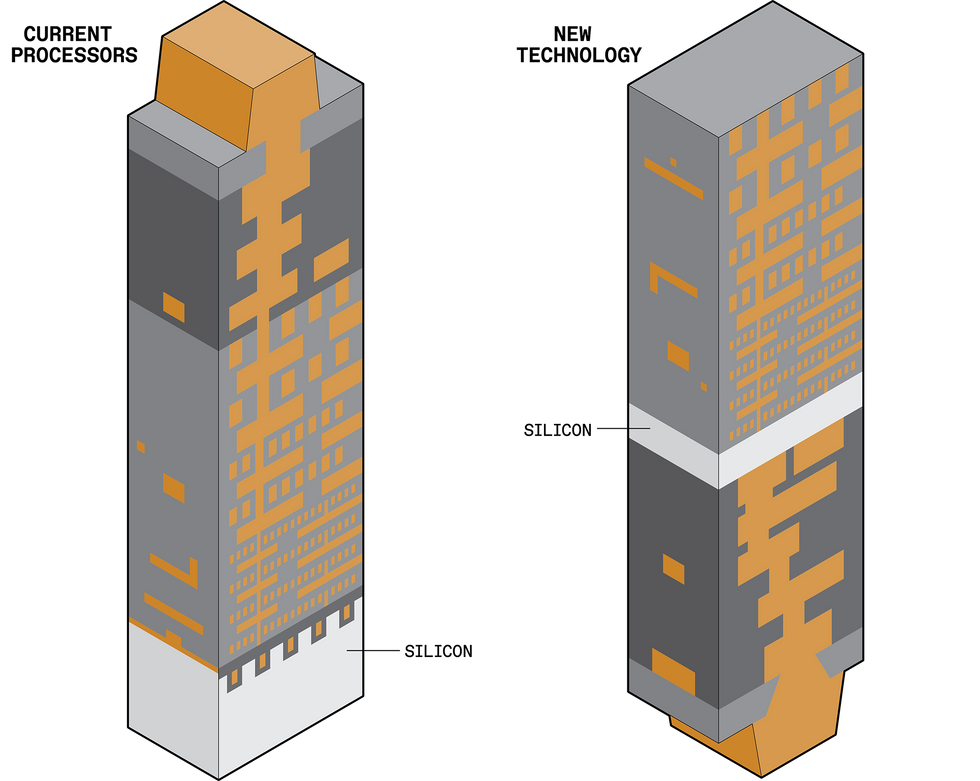
In modern processors each signals and power get to the silicon [gentle grey] from earlier mentioned. New technological innovation would separate people capabilities, saving power and earning far more space for signal routes [ideal].Chris Philpot
Fortuitously, we have a promising solution: We can use a side of the silicon which is extensive been ignored.
Electrons have to vacation a extensive way to get from the source that is generating them to the transistors that compute with them. In most electronics they vacation along the copper traces of a printed circuit board into a offer that holds the SoC, by way of the solder balls that join the chip to the
offer, and then by way of on-chip interconnects to the transistors by themselves. It’s this past phase that truly matters.
To see why, it aids to have an understanding of how chips are designed. An SoC starts as a bare piece of significant-quality, crystalline silicon. We first make a layer of transistors at the incredibly leading of that silicon. Next we backlink them collectively with metallic interconnects to type circuits with practical computing capabilities. These interconnects are shaped in layers referred to as a stack, and it can get a 10-to-20-layer stack to produce power and data to the billions of transistors on modern chips.
Those people layers closest to the silicon transistors are skinny and little in get to join to the tiny transistors, but they develop in dimension as you go up in the stack to bigger levels. It’s these levels with broader interconnects that are improved at providing power due to the fact they have less resistance.
Now, each power and signals get to transistors from a network of interconnects earlier mentioned the silicon (the “front side”). But escalating resistance as these interconnects are scaled down to ever-finer dimensions is earning that plan untenable.Chris Philpot
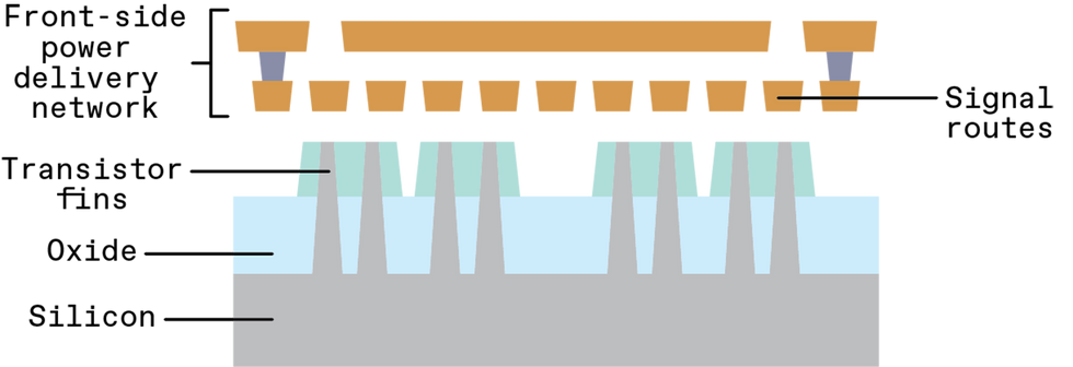
You can see, then, that the metallic that powers circuits—the power shipping and delivery network (PDN)—is on leading of the transistors. We refer to this as front-side power shipping and delivery. You can also see that the power network unavoidably competes for area with the network of wires that delivers signals, due to the fact they share the very same set of copper resources.
In get to get power and signals off of the SoC, we ordinarily join the uppermost layer of metal—farthest absent from the transistors—to solder balls (also referred to as bumps) in the chip offer. So for electrons to get to any transistor to do practical function, they have to traverse 10 to 20 layers of increasingly slim and tortuous metallic until they can at last squeeze by way of to the incredibly past layer of local wires.
This way of distributing power is essentially lossy. At every phase along the route, some power is dropped, and some will have to be utilised to handle the shipping and delivery alone. In modern SoCs, designers ordinarily have a finances that allows loss that prospects to a 10 percent reduction in voltage in between the offer and the transistors. Therefore, if we strike a full performance of ninety percent or better in a power-shipping and delivery network, our patterns are on the ideal keep track of.
Historically, these efficiencies have been achievable with superior engineering—some could even say it was effortless when compared to the difficulties we facial area now. In modern electronics, SoC designers not only have to handle escalating power densities but to do so with interconnects that are losing power at a sharply accelerating amount with each individual new generation.
You can structure a back again-side power shipping and delivery network which is up to seven instances as effective as the standard front-side network.
The escalating lossiness has to do with how we make nanoscale wires. That approach and its accompanying materials trace back again to about 1997, when IBM commenced to make interconnects out of copper alternatively of aluminum, and the field shifted along with it. Up until then aluminum wires had been fantastic conductors, but in a few far more steps along the
Moore’s Regulation curve their resistance would shortly be way too significant and become unreliable. Copper is far more conductive at modern IC scales. But even copper’s resistance commenced to be problematic the moment interconnect widths shrank beneath one hundred nanometers. Now, the smallest manufactured interconnects are about 20 nm, so resistance is now an urgent concern.
It aids to photograph the electrons in an interconnect as a complete set of balls on a billiards desk. Now picture shoving them all from one particular conclusion of the desk toward an additional. A few would collide and bounce in opposition to each individual other on the way, but most would make the journey in a straight-ish line. Now contemplate shrinking the desk by half—you’d get a ton far more collisions and the balls would shift far more slowly but surely. Next, shrink it all over again and maximize the amount of billiard balls tenfold, and you might be in anything like the scenario chipmakers facial area now. True electrons will not collide, essentially, but they get shut more than enough to one particular an additional to impose a scattering drive that disrupts the stream by way of the wire. At nanoscale dimensions, this prospects to vastly bigger resistance in the wires, which induces major power-shipping and delivery loss.
Growing electrical resistance is not a new obstacle, but the magnitude of maximize that we are viewing now with each individual subsequent approach node is unprecedented. On top of that, standard strategies of running this maximize are no lengthier an choice, due to the fact the production principles at the nanoscale impose so many constraints. Long gone are the days when we could arbitrarily maximize the widths of specified wires in get to overcome escalating resistance. Now designers have to adhere to specified specified wire widths or else the chip may not be manufacturable. So, the field is faced with the twin complications of bigger resistance in interconnects and less space for them on the chip.
There is an additional way: We can exploit the “vacant” silicon that lies beneath the transistors. At Imec, wherever authors Beyne and Zografos function, we have pioneered a production idea referred to as “buried power rails,” or BPR. The technique builds power connections beneath the transistors alternatively of earlier mentioned them, with the intention of producing fatter, less resistant rails and liberating area for signal-carrying interconnects earlier mentioned the transistor layer.
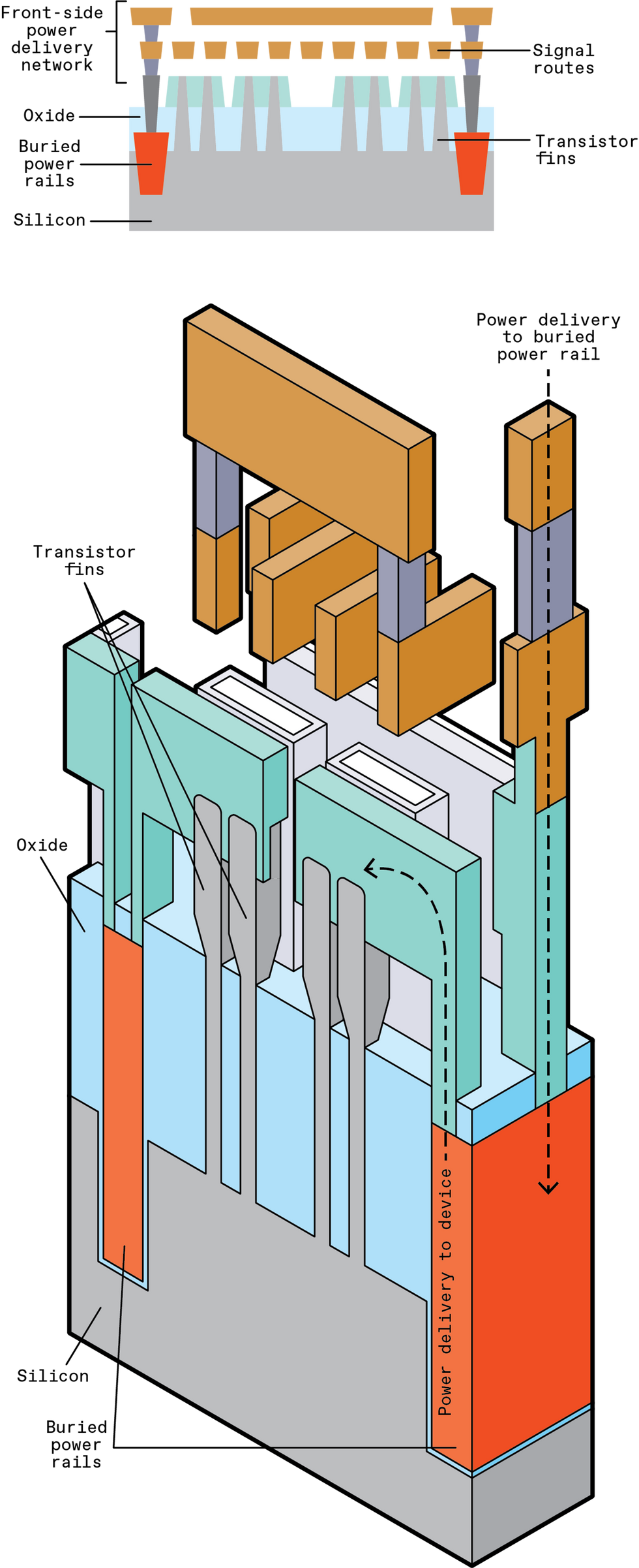
To minimize the resistance in power shipping and delivery, transistors will faucet power rails buried in just the silicon. These are relatively significant, very low-resistance conductors that numerous logic cells could join with.Chris Philpot
To construct BPRs, you first have to dig out deep trenches beneath the transistors and then fill them with metallic. You have to do this prior to you make the transistors by themselves. So the metallic option is critical. That metallic will need to withstand the processing steps utilised to make significant-quality transistors, which can get to about one,000 °C. At that temperature, copper is molten, and melted copper could contaminate the whole chip. We’ve for that reason experimented with ruthenium and tungsten, which have bigger melting points.
Considering the fact that there is so considerably unused area beneath the transistors, you can make the BPR trenches huge and deep, which is ideal for providing power. In comparison to the skinny metallic layers specifically on leading of the transistors,
BPRs can have one/20 to one/thirty the resistance. That usually means that BPRs will efficiently permit you to produce far more power to the transistors.
On top of that, by relocating the power rails off the leading side of the transistors you free of charge up space for the signal-carrying interconnects. These interconnects type elementary circuit “cells”—the smallest circuit units, these as SRAM memory little bit cells or straightforward logic that we use to compose far more intricate circuits. By working with the area we’ve freed up, we could shrink people cells by
16 percent or far more, and that could in the long run translate to far more transistors for each chip. Even if attribute dimension stayed the very same, we’d continue to force Moore’s Regulation one particular stage further.
Regretably, it seems like burying local power rails by itself will not likely be more than enough. You continue to have to convey power to people rails down from the leading side of the chip, and that will price tag performance and some loss of voltage.
Long gone are the days when we could arbitrarily maximize the widths of specified wires in get to overcome escalating resistance.
Researchers at Arm, including authors Cline and Prasad, ran a simulation on one particular of their CPUs and uncovered that, by by themselves, BPRs could permit you to construct a 40 percent far more effective power network than an ordinary front-side power shipping and delivery network. But they also uncovered that even if you utilised BPRs with front-side power shipping and delivery, the general voltage delivered to the transistors was not significant more than enough to maintain significant-functionality procedure of a CPU.
The good thing is, Imec was simultaneously creating a complementary solution to further strengthen power shipping and delivery: Move the whole power-shipping and delivery network from the front side of the chip to the back again side. This solution is referred to as “back again-side power shipping and delivery,” or far more normally “back again-side metallization.” It involves thinning down the silicon that is beneath the transistors to 500 nm or less, at which position you can create nanometer-dimension “by way of-silicon vias,” or
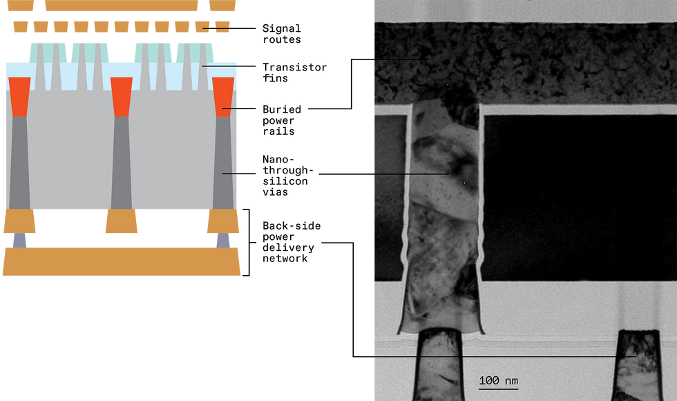
nano-TSVs. These are vertical interconnects that can join up by way of the back again side of the silicon to the base of the buried rails, like hundreds of tiny mineshafts. When the nano-TSVs have been produced beneath the transistors and BPRs, you can then deposit more layers of metallic on the back again side of the chip to type a complete power-shipping and delivery network.
Expanding on our earlier simulations, we at Arm uncovered that just two layers of thick back again-side metallic was more than enough to do the work. As extensive as you could area the nano-TSVs closer than 2 micrometers from each individual other, you could structure a back again-side PDN that was four instances as effective as the front-side PDN with buried power rails and seven instances as effective as the standard front-side PDN.
The back again-side PDN has the more edge of staying bodily divided from the signal network, so the two networks no lengthier contend for the very same metallic-layer resources. There’s far more space for each individual. It also usually means that the metallic layer attributes no lengthier need to be a compromise in between what power routes favor (thick and huge for very low resistance) and what signal routes favor (skinny and slim so they can make circuits from densely packed transistors). You can simultaneously tune the back again-side metallic layers for power routing and the front-side metallic layers for signal routing and get the ideal of each worlds.
Relocating the power shipping and delivery network to the other side of the silicon—the “back side”—reduces voltage loss even far more, due to the fact all the interconnects in the network can be designed thicker to decrease resistance. What’s far more, removing the power-shipping and delivery network from earlier mentioned the silicon leaves far more space for signal routes, primary to even scaled-down logic circuits and allowing chipmakers squeeze far more transistors into the very same spot of silicon.
Chris Philpot/IMEC
In our patterns at Arm, we uncovered that for each the standard front-side PDN and front-side PDN with buried power rails, we had to sacrifice structure functionality. But with back again-side PDN the CPU was capable to realize significant frequencies
and have electrically effective power shipping and delivery.
You could, of training course, be questioning how you get signals and power from the offer to the chip in these a plan. The nano-TSVs are the key below, way too. They can be utilised to transfer all input and output signals from the front side to the back again side of the chip. That way, each the power and the I/O signals can be hooked up to solder balls that are positioned on the back again side.
Simulation reports are a terrific start, and they display the CPU-structure-level potential of back again-side PDNs with BPR. But there is a extensive street ahead to bring these systems to significant-quantity production. There are continue to major materials and production difficulties that need to be solved. The ideal option of metallic materials for the BPRs and nano-TSVs is critical to manufacturability and electrical performance. Also, the significant-aspect-ratio (deep but skinny) trenches required for each BPRs and nano-TSVs are incredibly difficult to make. Reliably etching tightly spaced, deep-but-slim features in the silicon substrate and filling them with metallic is relatively new to chip manufacture and is continue to anything the field is having to grips with. Creating production resources and procedures that are responsible and repeatable will be necessary to unlocking prevalent adoption of nano-TSVs.
On top of that, battery-driven SoCs, like people in your telephone and in other power-constrained patterns, previously have considerably far more subtle power-shipping and delivery networks than people we’ve discussed so much. Modern-day power shipping and delivery separates chips into numerous power domains that can run at distinct voltages or even be turned off completely to conserve power. (See ”
A Circuit to Raise Battery Existence,” IEEE Spectrum, August 2021.)
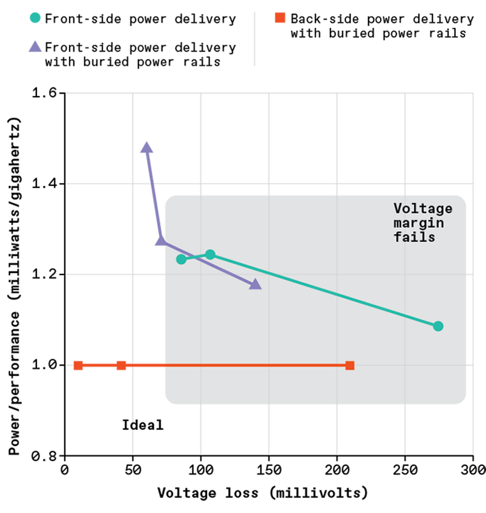
In exams of numerous patterns working with three varieties of power shipping and delivery, only back again-side power with buried power rails [pink] provides more than enough voltage without compromising functionality.Chris Philpot
Therefore, back again-side PDNs and BPRs are sooner or later likely to have to do considerably far more than just efficiently produce electrons. They are likely to have to exactly handle wherever electrons go and how many of them get there. Chip designers will not want to get numerous steps backward when it arrives to chip-level power structure. So we will have to simultaneously improve structure and production to make certain that BPRs and back again-side PDNs are improved than—or at least suitable with—the power-saving IC techniques we use now.
The potential of computing depends on these new production techniques. Electrical power use is vital no matter if you might be worrying about the cooling bill for a data centre or the amount of instances you have to charge your smartphone each individual day. And as we keep on to shrink transistors and ICs, providing power turns into a major on-chip obstacle. BPR and back again-side PDNs may well solution that obstacle if engineers can prevail over the complexities that come with them.
This posting appears in the September 2021 print concern as “Electrical power From Under.”


