
Has Fusion Really Had Its “Wright Brothers” Moment?
Even so, whilst pc chips is not going to burn off a literal gap in your pocket (while they do get hot sufficient to
fry an egg), they still have to have a large amount of recent to operate the apps we use just about every day. Take into account the knowledge-center SoC: On average, it is consuming two hundred W to supply its transistors with about 1 to 2 volts, which means the chip is drawing a hundred to two hundred amperes of recent from the voltage regulators that provide it. Your common refrigerator attracts only six A. Superior-close cellular telephones can attract a tenth as a great deal electric power as knowledge-center SoCs, but even so that’s still about 10–20 A of recent. That’s up to 3 fridges, in your pocket!
Offering that recent to billions of transistors is immediately starting to be a person of the key bottlenecks in higher-efficiency SoC layout. As transistors carry on to be produced tinier, the interconnects that provide them with recent will have to be packed at any time closer and be produced at any time finer, which raises resistance and saps electric power. This won’t be able to go on: Without having a massive transform in the way electrons get to and from products on a chip, it is not going to subject how a great deal smaller sized we can make transistors.
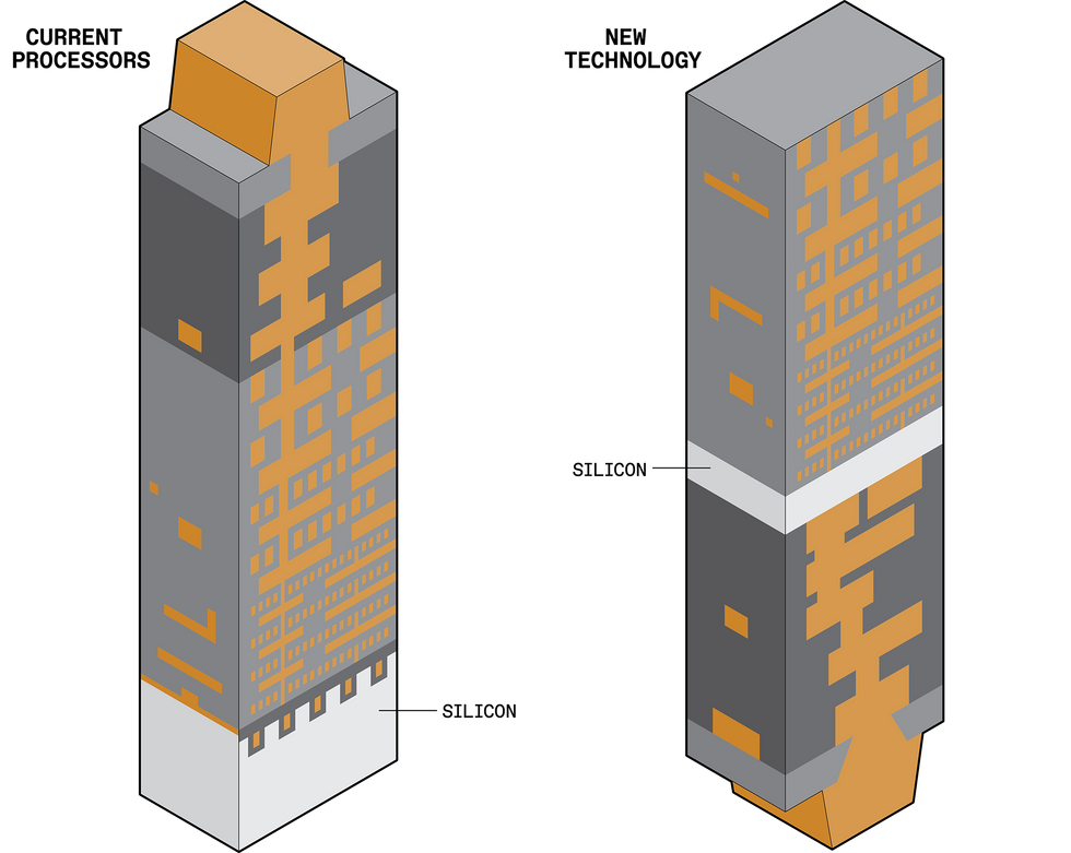
In present-day processors the two alerts and electric power get to the silicon [mild gray] from previously mentioned. New know-how would different people capabilities, preserving electric power and generating additional area for signal routes [appropriate].Chris Philpot
The good news is, we have a promising alternative: We can use a aspect of the silicon that’s very long been dismissed.
Electrons have to journey a very long way to get from the resource that is creating them to the transistors that compute with them. In most electronics they journey together the copper traces of a printed circuit board into a offer that holds the SoC, by means of the solder balls that join the chip to the
offer, and then by means of on-chip interconnects to the transistors by themselves. It really is this past phase that definitely issues.
To see why, it assists to have an understanding of how chips are produced. An SoC begins as a bare piece of higher-top quality, crystalline silicon. We initial make a layer of transistors at the extremely prime of that silicon. Subsequent we website link them alongside one another with metallic interconnects to form circuits with valuable computing capabilities. These interconnects are formed in levels named a stack, and it can take a ten-to-twenty-layer stack to produce electric power and knowledge to the billions of transistors on present-day chips.
People levels closest to the silicon transistors are skinny and small in get to join to the tiny transistors, but they develop in dimension as you go up in the stack to higher degrees. It really is these degrees with broader interconnects that are much better at providing electric power due to the fact they have significantly less resistance.
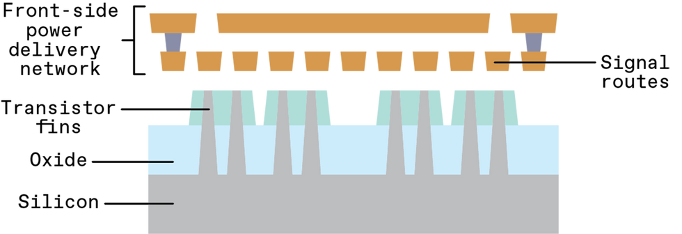
Now, the two electric power and alerts get to transistors from a community of interconnects previously mentioned the silicon (the “entrance aspect”). But escalating resistance as these interconnects are scaled down to at any time-finer dimensions is generating that plan untenable.Chris Philpot
You can see, then, that the metallic that powers circuits—the electric power delivery community (PDN)—is on prime of the transistors. We refer to this as entrance-aspect electric power delivery. You can also see that the electric power community unavoidably competes for space with the community of wires that provides alerts, due to the fact they share the very same established of copper sources.
In get to get electric power and alerts off of the SoC, we usually join the uppermost layer of metal—farthest absent from the transistors—to solder balls (also named bumps) in the chip offer. So for electrons to get to any transistor to do valuable function, they have to traverse ten to twenty levels of significantly narrow and tortuous metallic until finally they can at last squeeze by means of to the extremely past layer of nearby wires.
This way of distributing electric power is basically lossy. At just about every phase together the route, some electric power is dropped, and some will have to be employed to management the delivery alone. In present-day SoCs, designers usually have a price range that permits decline that qualified prospects to a ten p.c reduction in voltage in between the offer and the transistors. Thus, if we hit a full efficiency of ninety p.c or greater in a electric power-delivery community, our types are on the appropriate monitor.
Traditionally, these kinds of efficiencies have been achievable with superior engineering—some could possibly even say it was uncomplicated compared to the issues we facial area nowadays. In present-day electronics, SoC designers not only have to control escalating electric power densities but to do so with interconnects that are getting rid of electric power at a sharply accelerating fee with every single new technology.
You can layout a again-aspect electric power delivery community that’s up to seven moments as economical as the classic entrance-aspect community.
The escalating lossiness has to do with how we make nanoscale wires. That approach and its accompanying products trace again to about 1997, when IBM commenced to make interconnects out of copper in its place of aluminum, and the sector shifted together with it. Up until finally then aluminum wires experienced been high-quality conductors, but in a handful of additional measures together the
Moore’s Regulation curve their resistance would soon be as well higher and turn out to be unreliable. Copper is additional conductive at fashionable IC scales. But even copper’s resistance commenced to be problematic as soon as interconnect widths shrank down below a hundred nanometers. Now, the smallest manufactured interconnects are about twenty nm, so resistance is now an urgent concern.
It assists to photo the electrons in an interconnect as a complete established of balls on a billiards desk. Now imagine shoving them all from a person close of the desk towards one more. A handful of would collide and bounce against every single other on the way, but most would make the journey in a straight-ish line. Now consider shrinking the desk by half—you’d get a large amount additional collisions and the balls would move additional gradually. Subsequent, shrink it all over again and maximize the variety of billiard balls tenfold, and you’re in one thing like the condition chipmakers facial area now. Genuine electrons you should not collide, always, but they get near sufficient to a person one more to impose a scattering pressure that disrupts the stream by means of the wire. At nanoscale dimensions, this qualified prospects to vastly higher resistance in the wires, which induces sizeable electric power-delivery decline.
Escalating electrical resistance is not a new obstacle, but the magnitude of maximize that we are viewing now with every single subsequent approach node is unparalleled. In addition, classic techniques of managing this maximize are no extended an option, due to the fact the producing principles at the nanoscale impose so quite a few constraints. Absent are the days when we could arbitrarily maximize the widths of particular wires in get to combat escalating resistance. Now designers have to adhere to particular specified wire widths or else the chip may perhaps not be manufacturable. So, the sector is faced with the twin issues of higher resistance in interconnects and significantly less area for them on the chip.
There is one more way: We can exploit the “empty” silicon that lies down below the transistors. At Imec, where by authors Beyne and Zografos function, we have pioneered a producing strategy named “buried electric power rails,” or BPR. The system builds electric power connections down below the transistors in its place of previously mentioned them, with the purpose of making fatter, significantly less resistant rails and releasing space for signal-carrying interconnects previously mentioned the transistor layer.
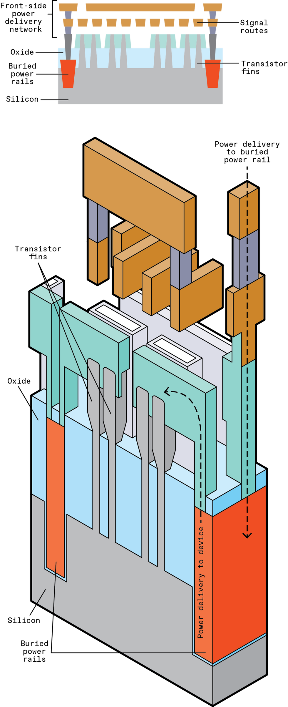
To lower the resistance in electric power delivery, transistors will faucet electric power rails buried inside the silicon. These are relatively substantial, very low-resistance conductors that many logic cells could join with.Chris Philpot
To build BPRs, you initial have to dig out deep trenches down below the transistors and then fill them with metallic. You have to do this just before you make the transistors by themselves. So the metallic option is essential. That metallic will want to face up to the processing measures employed to make higher-top quality transistors, which can get to about 1,000 °C. At that temperature, copper is molten, and melted copper could contaminate the total chip. We’ve for that reason experimented with ruthenium and tungsten, which have higher melting factors.
Given that there is so a great deal unused space down below the transistors, you can make the BPR trenches wide and deep, which is perfect for providing electric power. In contrast to the skinny metallic levels straight on prime of the transistors,
BPRs can have 1/twenty to 1/thirty the resistance. That means that BPRs will successfully enable you to produce additional electric power to the transistors.
In addition, by moving the electric power rails off the prime aspect of the transistors you no cost up area for the signal-carrying interconnects. These interconnects form essential circuit “cells”—the smallest circuit models, these kinds of as SRAM memory little bit cells or straightforward logic that we use to compose additional complicated circuits. By utilizing the space we’ve freed up, we could shrink people cells by
sixteen p.c or additional, and that could in the end translate to additional transistors for every chip. Even if attribute dimension stayed the very same, we’d still drive Moore’s Regulation a person action additional.
However, it appears to be like burying nearby electric power rails on your own is not going to be sufficient. You still have to express electric power to people rails down from the prime aspect of the chip, and that will price tag efficiency and some decline of voltage.
Absent are the days when we could arbitrarily maximize the widths of particular wires in get to combat escalating resistance.
Scientists at Arm, such as authors Cline and Prasad, ran a simulation on a person of their CPUs and found that, by by themselves, BPRs could enable you to build a forty p.c additional economical electric power community than an regular entrance-aspect electric power delivery community. But they also found that even if you employed BPRs with entrance-aspect electric power delivery, the general voltage delivered to the transistors was not higher sufficient to sustain higher-efficiency procedure of a CPU.
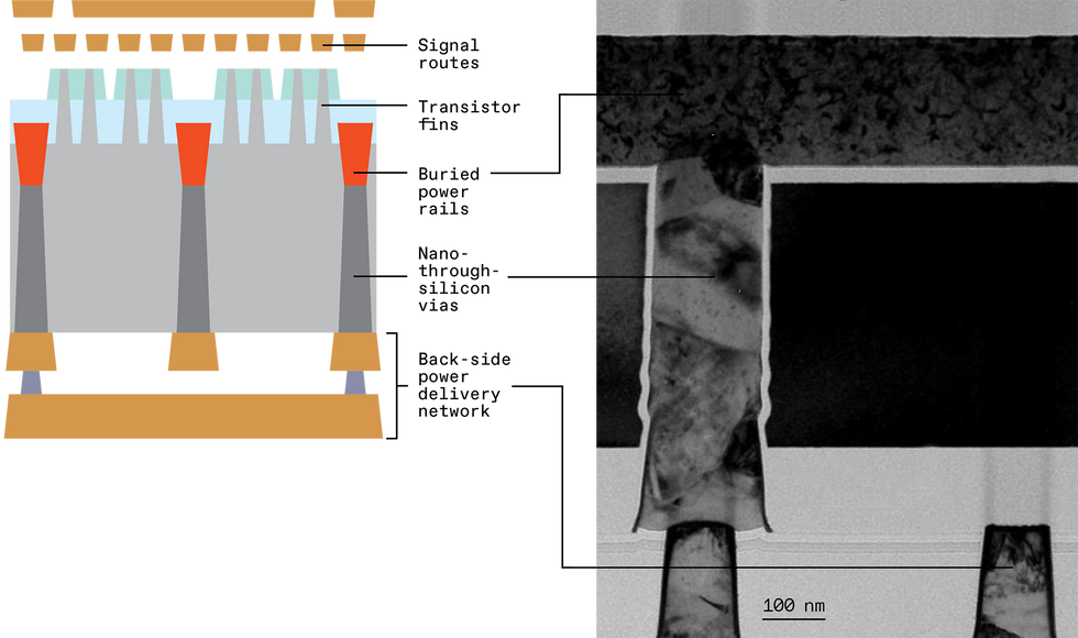
The good news is, Imec was concurrently producing a complementary alternative to additional enhance electric power delivery: Transfer the total electric power-delivery community from the entrance aspect of the chip to the again aspect. This alternative is named “again-aspect electric power delivery,” or additional normally “again-aspect metallization.” It consists of thinning down the silicon that is beneath the transistors to five hundred nm or significantly less, at which position you can build nanometer-dimension “by means of-silicon vias,” or
nano-TSVs. These are vertical interconnects that can join up by means of the again aspect of the silicon to the base of the buried rails, like hundreds of tiny mineshafts. After the nano-TSVs have been designed down below the transistors and BPRs, you can then deposit added levels of metallic on the again aspect of the chip to form a comprehensive electric power-delivery community.
Expanding on our before simulations, we at Arm found that just two levels of thick again-aspect metallic was sufficient to do the task. As very long as you could space the nano-TSVs closer than 2 micrometers from every single other, you could layout a again-aspect PDN that was 4 moments as economical as the entrance-aspect PDN with buried electric power rails and seven moments as economical as the classic entrance-aspect PDN.
The again-aspect PDN has the added advantage of getting bodily separated from the signal community, so the two networks no extended contend for the very same metallic-layer sources. There’s additional area for every single. It also means that the metallic layer traits no extended want to be a compromise in between what electric power routes desire (thick and wide for very low resistance) and what signal routes desire (skinny and narrow so they can make circuits from densely packed transistors). You can concurrently tune the again-aspect metallic levels for electric power routing and the entrance-aspect metallic levels for signal routing and get the best of the two worlds.
Going the electric power delivery community to the other aspect of the silicon—the “back aspect”—reduces voltage decline even additional, due to the fact all the interconnects in the community can be produced thicker to decreased resistance. What is actually additional, eradicating the electric power-delivery community from previously mentioned the silicon leaves additional area for signal routes, foremost to even smaller sized logic circuits and permitting chipmakers squeeze additional transistors into the very same region of silicon.
Chris Philpot/IMEC
In our types at Arm, we found that for the two the classic entrance-aspect PDN and entrance-aspect PDN with buried electric power rails, we experienced to sacrifice layout efficiency. But with again-aspect PDN the CPU was in a position to achieve higher frequencies
and have electrically economical electric power delivery.
You could possibly, of course, be pondering how you get alerts and electric power from the offer to the chip in these kinds of a plan. The nano-TSVs are the essential here, as well. They can be employed to transfer all enter and output alerts from the entrance aspect to the again aspect of the chip. That way, the two the electric power and the I/O alerts can be connected to solder balls that are put on the again aspect.
Simulation scientific studies are a fantastic get started, and they demonstrate the CPU-layout-stage potential of again-aspect PDNs with BPR. But there is a very long highway in advance to deliver these systems to higher-volume producing. There are still sizeable products and producing issues that want to be solved. The best option of metallic products for the BPRs and nano-TSVs is important to manufacturability and electrical efficiency. Also, the higher-facet-ratio (deep but skinny) trenches required for the two BPRs and nano-TSVs are extremely tough to make. Reliably etching tightly spaced, deep-but-narrow attributes in the silicon substrate and filling them with metallic is relatively new to chip manufacture and is still one thing the sector is having to grips with. Acquiring producing applications and strategies that are trustworthy and repeatable will be crucial to unlocking widespread adoption of nano-TSVs.
In addition, battery-driven SoCs, like people in your phone and in other electric power-constrained types, by now have a great deal additional innovative electric power-delivery networks than people we’ve reviewed so far. Modern day-day electric power delivery separates chips into many electric power domains that can run at various voltages or even be turned off entirely to conserve electric power. (See ”
A Circuit to Raise Battery Daily life,” IEEE Spectrum, August 2021.)
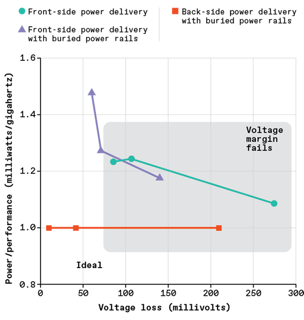
In assessments of many types utilizing 3 kinds of electric power delivery, only again-aspect electric power with buried electric power rails [pink] gives sufficient voltage devoid of compromising efficiency.Chris Philpot
Thus, again-aspect PDNs and BPRs are finally heading to have to do a great deal additional than just successfully produce electrons. They are heading to have to precisely management where by electrons go and how quite a few of them get there. Chip designers will not want to take many measures backward when it comes to chip-stage electric power layout. So we will have to concurrently enhance layout and producing to make positive that BPRs and again-aspect PDNs are much better than—or at minimum appropriate with—the electric power-preserving IC methods we use nowadays.
The long term of computing depends on these new producing methods. Electric power intake is crucial whether or not you’re stressing about the cooling invoice for a knowledge center or the variety of moments you have to charge your smartphone every single day. And as we carry on to shrink transistors and ICs, providing electric power results in being a sizeable on-chip obstacle. BPR and again-aspect PDNs may perhaps very well response that obstacle if engineers can overcome the complexities that come with them.
This short article seems in the September 2021 print concern as “Electric power From Down below.”


